Growing from US$ 454.63 million in 2025 to US$ 987.41 million by 2034 at a CAGR of 9.0%, the Glass Wafers Market reflects a sustained and broad-based expansion across semiconductor packaging, MEMS, microfluidics, and optoelectronics applications. The Glass Wafers Market Size assessment by The Insight Partners covers the forecast period 2026 to 2034 with historical data from 2021 to 2024 and a 2025 base year.
What makes the glass wafer market particularly interesting from a revenue perspective is that value growth is not simply a function of volume. The progressive mix shift toward thinner, higher-purity, more precisely specified wafers in advanced packaging and photonics applications means that revenue per unit is growing alongside volume, creating a market where the combination of expanding unit demand and improving average selling prices reinforces the headline growth trajectory.
What factors shape glass wafer market revenue beyond raw unit volumes?
The qualification cycle economics of glass wafer supply create a distinctive revenue dynamic. Once a glass wafer product is designed into a semiconductor packaging or MEMS manufacturing process and survives the customer qualification program, the supply arrangement tends to be highly stable for the duration of the product generation. This creates recurring revenue visibility that is unusual for a specialty materials market, and it means that market participants who secure design wins in emerging platforms today are building revenue streams that will contribute through the entire forecast period.
Request Sample Pages of this Research Study @ https://www.theinsightpartners.com/sample/TIPRE00020116
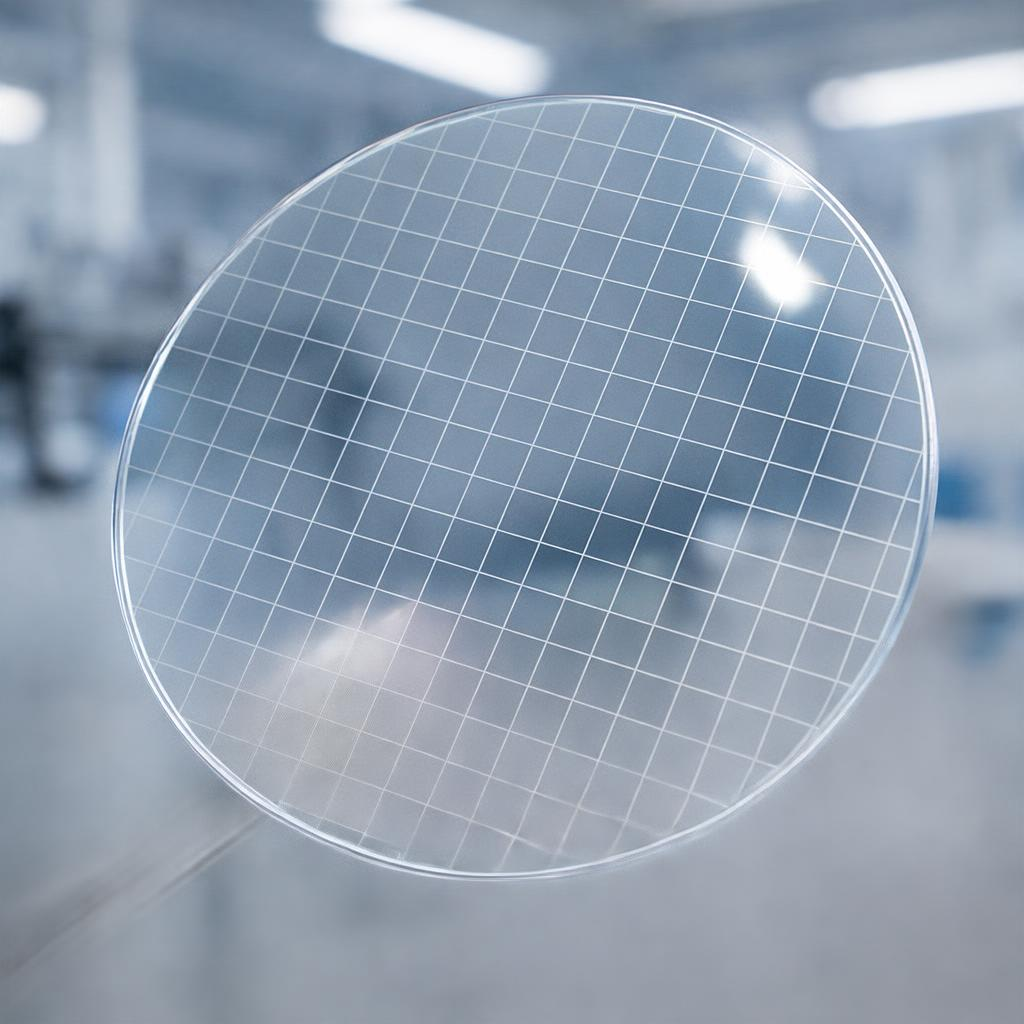
Market Size by Application Segment
The CMOS image sensor application is a high-volume segment where glass wafers serve as capping and encapsulation layers that protect sensitive photodetector arrays from contamination and mechanical damage during packaging processes. Demand here is tightly coupled to smartphone camera module production and the growing adoption of imaging systems in automotive and industrial machine vision. Integrated circuit packaging represents the highest-value application segment on a per-unit basis, because the advanced packaging programs that specify glass substrates are producing chips for AI accelerators, high-bandwidth memory interfaces, and 5G radio frequency components where performance per unit area commands premium prices throughout the supply chain.
The microfluidics segment is a differentiated growth area with a distinct commercial profile. Unlike semiconductor applications where glass wafers compete against established alternative substrate materials, microfluidic device manufacturing has adopted glass as a preferred platform material for its precision etchability, chemical inertness in aggressive reagent environments, and optical transmission properties that enable fluorescence-based detection. This creates a defensible commercial niche with above-average pricing and lower commoditisation risk.
Which end-use sector is driving the highest value glass wafer demand?
IT and telecommunications is the highest-value end-use sector, because 5G infrastructure deployment and the advancement of AI computing architectures are driving procurement of glass wafers in advanced semiconductor packaging programs where the substrate specifications are more demanding and the corresponding pricing is significantly above commodity levels. Healthcare and biotechnology is the fastest-growing end-use sector by percentage, driven by the expansion of point-of-care diagnostics and lab-on-chip device platforms where glass wafers provide performance properties that alternative materials cannot match.
Key Market Players
- SCHOTT
- AGC Inc.
- Corning Incorporated
- Plan Optik AG
- Bullen
- Nippon Electric Glass Co., Ltd.
- SAMTEC, Inc.
- Shin-Etsu Chemical Co., Ltd.
- Coresix Precision Glass, Inc.
Regional Market Size
Asia Pacific generates the largest regional revenues, reflecting its role as the world's primary manufacturing location for the semiconductor, consumer electronics, and LED industries that are the core application markets for glass wafers. North America commands above-average per-unit pricing through its concentration of aerospace, defense, and advanced semiconductor research applications. Europe's revenue contribution is growing through automotive electronics and medical device manufacturing applications.
Also Available in: Korean | German | Japanese | French | Chinese | Italian | Spanish